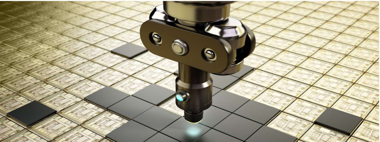
Die bonding
Die bonding, also known as die attach, is a crucial process in semiconductor manufacturing where a semiconductor chip, known as a die, is attached to a substrate or package. Die bonding ensures proper alignment and connection of the chip’s electrical contacts to the corresponding connections on the substrate, enabling the functionality of the semiconductor device. This process is essential for creating integrated circuits and other electronic components used in various devices, such as microprocessors, memory chips, and sensors.
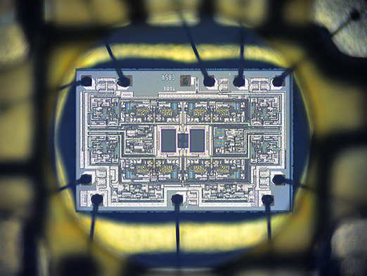
Wire bonding
In order to achieve a high bond yield, parameters such as bond force and bond time must be optimised. This allows to achieve strong and reliable bonds while minimising defects such as bond voids, cracks or delamination.
For several decades, wires have been used to connect semiconductor devices to their package or substrate, and as semiconductor devices become smaller and more complex, wire bonding faces the challenge of achieving high-density interconnections and fine-pitch bonding without a massive increase in process time.
Motion control
- AccurET
- ACCURET+
Do not hesitate to contact us to find out more about ETEL’s innovative and precise solutions.
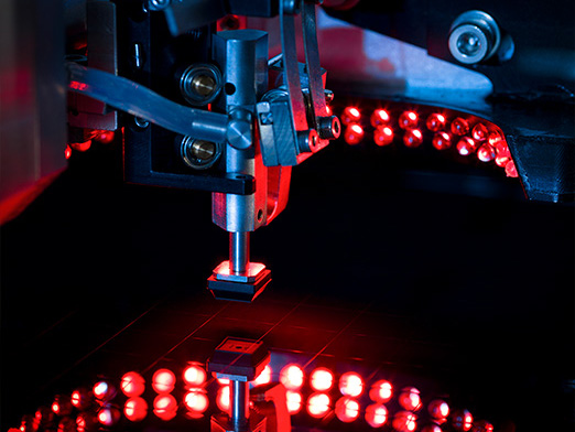
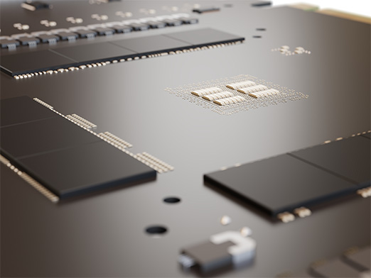
Flip chip die bonding
Flip-chip bonding enables a smaller interconnection pitch and therefore requires more precise alignment and registration between the semiconductor chip and the substrate.
In flip-chip bonding, the active side of the semiconductor chip is bonded directly to the substrate or packaged using solder bumps. In this technique, the semiconductor chip is flipped over, hence the name, and its active side faces the substrate.
ETEL has developed measurement strategies to decouple the force from the metrology and ensure a high throughput motion system without compromising precision, which is not affected by the thermal stress resulting from the high throughput requirement.
Motion systems
- TELICA : Our high duty dual gantry solution
Motion control
- AccurET 400
Do not hesitate to contact us to find out more about ETEL’s innovative and precise solutions.
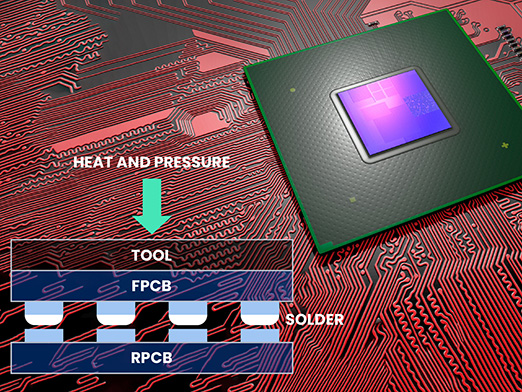
Thermo-compression bonding
Thermo-compression bonding (TCB) is another semiconductor packaging technique that demands precise control over temperature and pressure.
Transitioning between force and position control during thermal compression bonding is crucial to achieve a repeatable collapse while avoiding solder bridges between the interconnects.
ETEL has developed many macro functions hosted by the controller to allow perfect collapse control and ensure highest process performance.
Motion systems
- TELICA : Our high duty dual gantry solution
Motion control
- AccurET 400
Do not hesitate to contact us to find out more about ETEL’s innovative and precise solutions.
Hybrid bonding
Hybrid bonding, also known as direct bonding, is an advanced semiconductor packaging technique that offers several advantages but also presents unique challenges.
The absence of solder bumps allows to reach extremely high interconnect densities driving the process repeatability requirement to the level of front-end application. In die to wafer hybrid bonding, the common denominator is the die. This drives the need of a back-end application throughput.
For that combination of high accuracy and high throughput, ETEL is developing custom motion systems and control architectures for the most stringent applications.
Motion systems
- TELICA : Our high duty dual gantry solution
Motion control
- AccurET 400 : The high duty motion controller for pin point accuracy applications.
- Accuret VHP : Low noise position controller
For custom systems, please contact your sales representative.