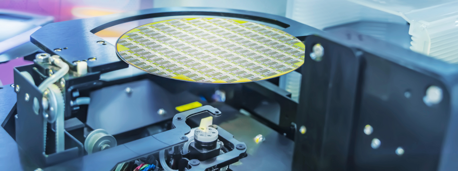
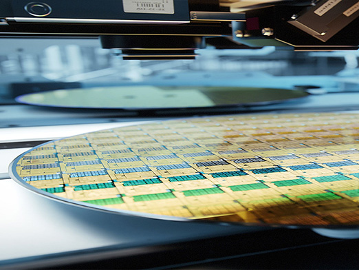
Wafer process control
When it comes to wafer processing, maintaining optimal performance throughout the production process is essential to ensure the quality and reliability of the semiconductor devices. Any deviation or error can lead to device failure and yield loss. This emphasises the importance of high-performance wafer process control from start to finish.
Overlay metrology
In the complex world of semiconductor production, overlay metrology presents a particular challenge. Misalignment can lead to costly failures. ETEL introduces innovative solutions to help you identify these accurately.
The increasing demand for smaller node sizes reinforces the need for pinpoint accuracy in layer alignment. Misalignment can lead to short circuits or connection errors, resulting in a non-functional chip. Therefore, they must be identified accurately and as early as possible in the chip manufacturing process to limit impact on fab yield and profit margins.
The growing pattern density leads to a reduction in error budgets and creates significant challenges in meeting total measurement uncertainty (TMU) requirements.
Consequently, it is of the utmost importance to ensure that the process is precise and robust. While improvements to the optical setup and the addition of software solutions such as image processing algorithms and AI are essential for success, they will never fully compensate for suboptimal substrate positioning.
ETEL offers a wide range of solutions that ensure first-class positioning accuracy and minimise both settling times and vibration transmission to the optics at maximum dynamics.
Motion systems
- CHARON2: Our most cost-effective architecture
- CHARON2HD: For the highest dynamics
- QUIET: To reduce settling time and increase machine throughput, minimize vibrations migrating to the optics, both from floor and from moving masses
Motion control
- ACCURET+: Mapping functions with increased position accuracy allowing optics fields of view optimization and reduced signal to noise ratio for a better position stability.
Do not hesitate to contact us to find out more about ETEL’s innovative and precise solutions.
Thin film metrology
Top notch chip manufacturing requires stable measurement conditions. ETEL offers innovative solutions to adapt to harsh topographies in angstrom-level thin film metrology.
Wafer warpage and shallow defect detection are only a few of the hurdles in thin film metrology. Even slight deviations from the optimal process plane can alter measurements, potentially leading to defect misidentification and a decline in overall production yield.
ETEL is developing multi-degree-of-freedom motion systems and mapping solutions to erase most of the motion systems static errors.
This minimizes deviations from the optimal process plane and ensures maximal process stability. Furthermore, these techniques can be applied to compensate uneven chuck or wafer topographies, elevating process performance to a new level.
Motion systems
- CHARON2: Our most cost-effective architecture
- VULCANO2: For higher duty-cycles
- METIS: Our air bearing motion system
- Z3TM+: For motion systems with up to 6 DOF tool point control
Motion control
- AccurET: Mapping functions with increased position accuracy allowing optics fields of view optimization and reduced signal to noise ratio for a better position stability.
- ACCURET+: Our new generation of electronics with even higher SNR and many new features
Do not hesitate to contact us to find out more about ETEL’s innovative and precise solutions.
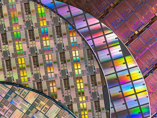
Critical dimension metrology
Distinguishing true deviations from process variability is crucial. ETEL can assist reducing your total measurement uncertainty (TMU) by improving image registration.
Next generation devices require complex designs with smaller pitches and more features. Ensuring the correct size and precise position of all geometries is essential for device functionality. As accuracy increases, the field of view shrinks, so more images are needed to cover the same area. Non-planar surfaces and 3D geometries require images at different heights, making it difficult to understand geometric relationships.
ETEL offers a diverse range of solutions ensuring top-notch position accuracy, advanced trigger functions, and providing actual trigger coordinates to minimize registration uncertainty and secure TMU.
Motion systems
- CHARON2: Our most cost-effective architecture
- VULCANO2: For higher duty-cycles
- METIS: Our air bearing motion system
- Z3TM+: For high bandwidth focus control
Motion control
- AccurET: Advanced trigger function
- ACCURET+: Our new generation of electronics with even higher SNR and many new features
Do not hesitate to contact us to find out more about ETEL’s innovative and precise solutions.
Defect inspection/review
Sub-micron defects can have a significant impact on device performance and can occur anywhere on a wafer. To ensure optimal product quality, large quantities of wafers must be subjected to extensive inspections quickly and efficiently.
Detecting and classifying different types of defects requires advanced inspection techniques that are able to distinguish between normal deviations and real defects. Maximising stability during inspection is key to ensuring process quality and enabling accurate classification.
ETEL offers solutions that combine high dynamics with extremely short settling times to minimise the time for moving and measuring (MAM).
Motion systems
- VULCANO2: For higher duty-cycles
- QUIET: To reduce settling time and increase machine throughput, minimize vibrations migrating to the optics, both from floor and from moving masses
Motion control
- AccurET: Wide range of electronics
- ACCURET+: Our new generation of electronics with even higher SNR and many new features
- UltimET: Our motion controller with acceleration feed-forward and many other advanced features
Do not hesitate to contact us to find out more about ETEL’s innovative and precise solutions.