
TELICA
TELICA, a cutting-edge multi-axes platform, is revolutionizing semiconductor back-end applications with its dual gantry architecture, offering unmatched accuracy and throughput for advanced die bonding applications and more.
TELICA is a multi-axes platform designed for semiconductor back-end applications, featuring a dual gantry architecture that offers motion along four degrees of freedom (X, Y, Z, and Rz) with a total of eight controlled axes. This advanced design supports demanding processes such as Flip-chip, Fan-out, Hybrid bonding, 2.5D/3D packages, µ-LED bonding, and dispensing applications. TELICA excels in both high positioning accuracy and high throughput, achieving ±1 µm global placement accuracy and ±350 nm local accuracy at a throughput of 10 kUPH for typical flip chip die bonding applications. For µ-LED bonding, it reaches up to 180 kUPH.
TELICA introduces a novel metrology approach that significantly reduces the Abbé errors and the relative positioning mismatch between the process tool and substrate. Multi-dimensional encoders located at process plane level ensure precise placement, while water-cooled ironcore motors enable extreme duty cycles. Coupled with ETEL’s advanced AccurET controllers, TELICA benefits from features like zero settling time, advanced feedforward and trajectory filters, full synchronization of all axes with nanosecond jitter, and comprehensive software diagnostic and system identification tools for control optimization.
Bidirectional repeatability
Position stability
Dynamics
Characteristics
- ±350 nm local placement accuracy (moves with local alignment) at 10 kUPH throughput.
- ±200 nm local placement accuracy (moves with local alignment) at 2 kUPH throughput.
- ±1 µm global placement accuracy (blind moves).
- <10 minutes thermal transient (from cold start to hot working state).
- Up to 10 kUPH throughput for a typical flip chip die bonding application.
- Up to 2 kUPH throughput for a hybrid bonding application.
- Up to 180 kUPH throughput for µ-LED bonding.
- Up to 4 g acceleration in X, 6 g in Y and 7.5 g in Z.
- Up to 2 m/s speed in X and Y and 1 m/s in Z.
- ISO 5 cleanroom compatible.
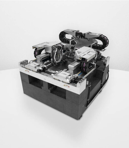
Multi-axes platform TELICA
Here are the key features of our models:
Provides precise motion along four degrees of freedom.
Achieves ±1 µm global placement accuracy and down to ±200 nm local accuracy.
Available with one or two gantry beams depending on performance requirements.
Secondary metrology loop at process plane level limiting Abbé errors and chip to substrate relative positioning mismatch.
Enable extreme duty cycles for demanding applications.
Offer advanced control features for optimized performance.